
| Contents |
| Dragon HW |
| Dragon SW (DDOS) |
| Dragon SW (OS9) |
| Dragon Projects |
PIA Based RAM Disc
Up2Date '93
Back in several issues ago, I finished covering address decoding for the Dragon, enabling a number of (up to) 4 byte devices to be mapped into the I/O area at $FF10 & $FF30. These devices are enabled by a 74HC138 decoder chip which provides 8 P2~ type decode outputs for I/O devices. Such straightforward devices, as I have previously mentioned are 68XX compatible peripherals ie. the 6821 PIA or 6850 ACIA which can be attached relatively easily. However, it is not impossible to attach other devices which are not specifically designed to be 68XX compatible. (An example was shown in issue 7 where a standard buffer chip was used).
First, some of the problems involved in adding more memory. In this instance, it helps to compare this with the different forms of PC memory (for those that understand their expanded from extended memory). The Dragon can be compared to the old 8086 based PCs (an insult I know!) where the processor could only physically address 1 megabyte. This is because there is not enough address lines on the processor to output a figure higher than 1 megabyte in binary (20 bits). On the Dragon, with a 16 bit address bus this is limited to 64K. When applications increased in size on the PC, a way had to be found to give the machines more memory. This was achieved by allocating 64K of the machines memory as a 'window' to the extra RAM. The extra memory (as much as possible, though it was usually in the region of 256K) could be 'paged' in and out of the window and the idea of expanded memory was born. A standard was formed (EMS) and with a special memory manager loaded which dealt with the paging, applications which recognized EMS could use this memory as data storage. Once the 80286 & 386 processors arrived which could address more than 1MB, this was no longer required however a good many programs still use EMS as extra memory. Back on the Dragon front, the 68000+ processor was the next generation processor which could access more than 64K. In order to access more than 64K it would be necessary to set up some sort of page frame in the Dragon's memory. The Plus board implemented this to a degree using 32K pages which it swopped in and out of the main memory. A good area to use could be the 8K unused space above the DOS cartridge as a frame without upsetting the machine too much. However, the problem with this is the work involved in mapping the memory in properly (plus on D64s you cannot write to the cartridge memory) and the fact that no such EMS standard exists, meaning that no existing software could use your extra memory only software you had written. A better method, and one which the plus board utilises was that of a RAM drive.
A RAM drive is a section of memory designed to mimic a disc drive. That is, files are created and stored on it exactly like on a disc. The advantage is that it is much faster and enables existing software to use it without modification. Newcomers to the Dragon disc system will find it infinitely faster than using tape, however when dealing with multi-loader programs such as KCS's Desktop Publisher and OS9 users (particularly C and Pascal compilers which do a lot of disk I/O) it can suddenly seem quite slow. Also, the system does alarming things with interrupts when using the disc drives.
Attempting to send files down the serial port under OS9 is almost impossible from disc because the control lines are continuously being altered by the disc controller. Even though the RAM has been setup to mimic a disk drive, you can still use it like EMS as data storage if you write programs that can recognize and handle it. It may be worth writing a memory manager which your own programs can simply call and ask for data to be passed to & from the extra RAM. One of the uses I have put mine to is through in the recording, storage and playback of audio samples which I outlined in Issue 7.
64K is very limiting on the length of samples which can be stored and it also prevents any significant interface to the user as program code needs to be kept to a minimum. By using extra RAM to store the samples, sounds of a much longer duration can be sampled & stored whilst freeing up the main memory for an easy to use interface for the user.
The RAM disc I have setup maps into one of the 4 byte IO areas. It is designed specifically to be sector accessed like a disc. It allows for up to 32MB of memory to be addressed (somewhat excessive I know!) via a 24 bit address bus. First you tell it the which upper 16 bits you wish to address by passing it in 2 8 byte chunks. Then, you consecutively read or write to one location 256 times (the length of a standard sector - effectively addressing all of the lower 8 bits of the address in turn).
The way it is set up makes it easy to use where logical sector numbers (LSNs) are specified. This is a system where by disk sectors are numbered continuously from 0 upwards instead of by track/sector. Therefore on a standard Dragon disk, LSN 0 is Track 0, sector 1 and LSN 19 is Track 1, sector 1 etc. Therefore, you simply pass the LSN as the upper 16 bits of the address to the RAM drive and read or write the data.
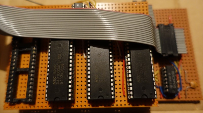
A couple of general points before I start on how to begin building the RAM board. First, although the design is relatively straight-forward, it is major job to wire up, mostly because of all the address lines involved. A lot of mine was done using wire wrap, mostly to keep the volume of wires down. The design interfaces to the processor through an MC6821 PIA.
My preference would be to connect it directly to the processor's bus, but at the time of building mine there was insufficient (and still is!) room internally on my Dragon and it had to sit outside on a length of ribbon cable, which is far too long for the processor signals to travel.
There are a few advantages in using this method, it makes testing easier and it can be attached to any expansion card which has PIA on it (Maplin did one a few years back which could be utilised). With a few modifications it could be adapted fairly easily to connect directly to the processor's bus, and would therefore be slightly faster. It uses the 'A' side of the PIA as the data/address bus and the 'B' side as the control bus. Four lines are used on the B side:
PB0 -> MSA (Most Significant Address bits 15-23)
PB1 -> RS  (Register Select)
PB2 -> R/W (Read & Write - not processor R/W)
PB3 -> LSA (Least Significant Address bits 8-15)
(see issue 5 of UP2DATE for details on connecting up a PIA).
I have chosen Static RAM to use for the main storage instead of Dynamic which the Dragon uses. Although slightly cheaper, it avoids the refresh circuitry and is easy to connect up. It can also be easily battery backed up. The device I used was a 431000 1Mbit SRAM providing 128K of memory. Whilst this is quite a lot of memory in Dragon terms, it soon goes and I currently have 2 devices providing 256K. Each device is about £25.
In addition to this, the other devices required are a 74HC00 Quad 2 i/p NAND gate, a 74HC08 Quad 2 i/p AND gate, 2 * 74HC373 Octal Latch, and a 74HC393 Dual 4-bit binary counter. In addition, you will also need a 74HC138 3 to 8 decoder if you wish to use more than 128K.
The decoding centres around the two logic chips NAND & AND. The PIA is setup such that whenever data is read from the A side, it's strobe line CA2 goes low (if data is written, the software needs to do a 'dummy' read afterwards to ensure the CA2 line goes low). First, a NAND gate is used as an invertor to flip the CA2 line so when data is strobed it goes high instead of low.
In order to select which address you wish to read or write to in the RAM chip, first the MSA line on port B should be set high. Then the upper 8 bits of the address (bits 16-23) are output on port A (followed by the 'dummy' read). CA2 is ANDed with MSA so when both signals are high, one of the 373 latches is enabled. The data on port A of the PIA is then read into the latch. A similar situation exists for the next lower eight bits of the address (bits 8-15). The LSA signal is again decoded with the CA2 line and data read into the other latch. In addition, when LSA is set the 393 counter is cleared to 0 by the MRA & MRB lines.
Once the address is written, 256 bytes of data can now be consecutively written to port A. First the RS line is set high. This is inverted through another NAND gate and used as chip select for the RAM chip. In addition RS is also ANDed with CA2 and fed to the CPa pin (pin 1) on the 393. The 393 is comprises two 4 bit counters, which are coupled together to provide one 8 bit counter (0-255). Every CPa is pulsed, the counter increments by 1.
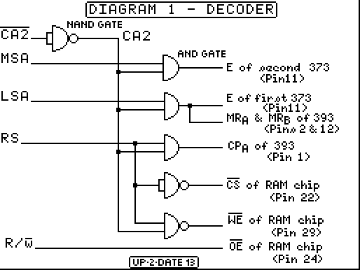
The RS signal is also NANDed with CA2 and fed to the WE (Write Enable) pin on the RAM chip. This ensures that the RAM chip only reads data on port A when it is valid. The R/W signal from port B is connected directly to OE (Output Enable) on the RAM chip, used to select whether data is to be read or written to the chip. When R/W is high data is pulsed into the chip via WE. When it is low, WE is ignored and the chip places the contents of the RAM onto its output pins.
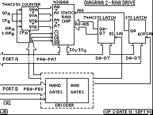
The bulk of the connections concern the routing of the RAM chip's data & address bus. The 8 lines from port A are connected to the RAM chips I/O1 to I/O8 lines, and to the inputs of both 373 latches (D0-D7). The outputs of these latches form the upper part of the address bus.
Connect the outputs of the first latch (the one controlled by the LSA signal) Q0-Q7 to the A8 to A15 lines on the RAM chip. OE on both 373 chips should be permanently tied to 0V. Only 1 output of the second latch is needed for 128K - Q0 should be connected to A16 of the RAM chip. The outputs of the 393 counter form the lower 8 bits of the RAM chips address.
Connect Q0a-Q3a to A0-A3 on the RAM chip, and Q0b-Q3b to A4-A7 on the RAM chip. In addition connect Q3a to CPb, to clock the other side of the counter. As data is successively written/read to port A of the PIA, the counter increments the addresses on the RAM chip.
That just about completes the board - the remaning CE2 line on the RAM chip being tied to +5V. Diagram 2 shows a block diagram of the finished board - I have not shown every individual signal as it would be far too complicated. The block diagram also roughly shows the stripboard layout I followed to build it.
Adding More Memory
Whilst 128K of extra RAM can seem at first more than adequate for most Dragon users, after a while it soon fills up, particularly when used as a disk drive. Under OS9 for example, running the Pascal compiler from RAM ONLY makes a substantial difference, however it will only just fit into 128K with a small amount left over for the source program itself. The C compiler will not fit into 128K at all.
However, the RAM board was designed to be expanded, as previously mentioned it can physically address up to 32MB so it is not too difficult to add more chips. If you are going to do this, it is worth considering early on how many you wish to add, so the extra sockets can be put in one go using wire wrap. All but one of the pins on the RAM chips need to be daisy chained together, the omitted pin being pin 22, CE.
This can be done relatively easily using wire wrap, by simply linking all the respective pins on the chip sockets together before soldering. However, attempting to do so after 1 socket has been soldered is difficult. If this is the case, the best way forward is to use a piggy back board arrangement.
An extra board needs to be made with as many RAM chip sockets on it as required, all linked together, except the last one. This needs to be a wire wrap socket, which then plugs into the originally socket on the lower board.
Each RAM chip now needs its only CE signal conneted. To do this, use a 74HC138 decoder, this will provide decode outputs for up to 8 128K chips - which should be more than adequate. Re-route the original CE signal from the first RAM chip to the E1 (pin 4) of the 138.
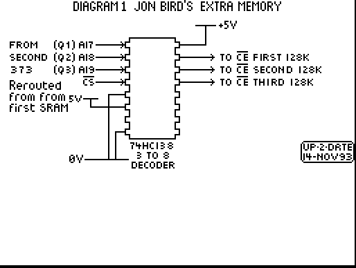
Connect the other E lines so they are permanently enabled (E2 to 0V & E3 to +5V). Some additional address lines from the second 373 latch are required to provide A17-A19 (Q1 to Q3 from the MSA decoded latch). These should be connected to the A0 to A2 lines on the 138 (pins 1 to 3). The 8 outputs of the 138 now provide the chip selects for the 128K RAM chips - 0~ (pin 15) for the first 128K, 1~ (pin 14) for the next 128K etc.
The board is designed to drive 128K RAM chips - the largest commercially available memories I can find. However, it probably won't be long till 256K & higher chips are available and it shouldn't be too difficult to connect these as well! Furthermore, with the addition of some refresh circuitry, it could be possible to use DRAM and the SIMM modules that PCs use which would really bump up the RAM at a cost which is significantly cheaper than SRAM.
The SRAM version could also be fairly easily battery backed up, enabling data stored on it to be retained after the machine had powered down. Adding enough chips could provide the equivalent of a small hard drive - with high access rates.
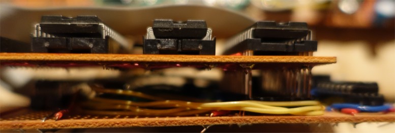
As I hinted at earlier, it's best to allow for the inclusion of any additional chips you think you will need. I didn't and to accomodate more than 128K of memory, created this piggy back arrangement. The board allowed for 4 devices, ultimately I fitted three of them.
Software
The software to work with the RAM drive should work at a sector level. That is the operating system should pass the sector requested to your controlling software which should then convert it into LSNs (if it is not already) and then transfer the data to/from the required location in RAM.
How this interfaces with the operating system is dependant on which system it is running under. Under a standard DragonDOS system, you could attempt one of two things.
First, write some additional commands dedicated to using the RAM drive (maybe the RAM Drive program reviewed in UPDATE could be adapted). The second method, and this method is limited to Dragon 64 users is to copy all the ROMS to RAM and patch the Basic disk operation processor vectored at [$C004].
This could be altered to recognize an access to an unused drive - for example drive 4 and pass this onto the RAM disc driver to handle. However, it is under the advanced Dragon operating systems OS9 & Flex that the RAM drive becomes really useful.
Under OS9, which I have the most experience in, it is a straighforward matter to write a disk driver & descriptor for the RAM drive. OS9 will pass to the driver the LSN it wishes to access, and this is then passed straight to the RAM board without any further calculation.
For now, back to patching DragonDOS. Principally, there are 4 types of operation that a disk controller will perform: read sector, write sector, seek sector & format track. Hence, you will need to write routines to accomplish this on your RAM drive. I will outline these routines for the patched disk command processor I mentioned earlier, the basic routines can then be copied for any other system you wish to implement it on.
The Disk operation processor performs 8 operations based on data in 14 bytes of memory at address $EA. The code in location $EA reflects the operation the disk processor is to perform:
0 = restore drive to track 0. This is equivalent to a seek to track 0, sector 1.
1 = seek track. Moves the disk head to the track specified in location $EC and sector in $ED. Our routine must therefore translate the track/sector combination to an LSN and move to that location in RAM.
2 = read sector. This reads the current sector into a buffer pointed to by $EE:EF. Our routine must therefore copy 256 bytes from RAM into the specified location.
3 = write sector & verify if flagged. This writes the data pointed to by $EE:EF to the current sector and verifies it if VERIFY ON. Our routine should copy the data in the buffer to RAM. No verify is needed as it should be impossible to corrupt memory...
4 = write sector, no verify. See 3. 5 = write track (format). Our routine can ignore format as it has no meaning - the RAM can already be written to and read from.
6 = read address of track. Probably used by format, and can be ignored?
7 = read sector to verify and leave the first two bytes in locations 79, 80. Can be done through routine 2.
Having covered the basic routines required to access to RAM drive, they can be written one by one. Using the following set of definitions, I have outlined them:
*RDISK V1.0 - (C)1992 BY J.BIRD
*RAM DISK FOR DDOS
*EQUATES:   - PIA control register codes follow:
DDR EQU 56  - for Data Direction Register
OFF EQU 60  - to switch 'A' side off
ACT EQU 44  - to activate 'A' side & CA2 strobe
EXTMSR EQU 1 - code to select MSA line on 'B'
READ EQU 2  - code to select RS (RAM) for read
WRIT EQU 6  - code to select RS & R/W for write
EXTLSR EQU 8 - code to select LSA line
OUT EQU 255 - to set PIA DDR for output
OUTB EQU 15 - to set PIA B side DDR 4 lines o/p
IOA EQU $FF34 - address of I/O location 'A'
CRA EQU $FF35 - address of Control Register 'A'
IOB EQU $FF36 - address of I/O location 'B'
CRB EQU $FF37 - address of Control Register 'B'
LSN RMB 2     - workspace to store LSN number
This is the setup for a PIA based at location $FF34 - the address at IOA-CRB should be changed to reflect where your PIA is mapped.
0 - Restore to track zero
The restore routine sets LSN to zero and calls the seek routine.
*RESTORE - SET LSN TO 0000
RESTORE CLR LSN
CLR LSN+1
BRA SEEK
1 - Seek to LSN
This will set the address up in SRAM, by loading the LSN into the two 373 latches.
*SEEK - MOVE TO SECTOR IN RAM
SEEK LDA #DDR
STA CRA        - set A side to data direction
LDA #OUT
STA IOA        - enable A for output
LDA #ACT
STA CRA        - set control reg for CA2 strobe
LDA #EXTMSR
STA IOB        - set the MSA line on port B
LDD LSN        - D = 16 bit logical sector num.
STA IOA        - write the MSB into port A
LDA IOA        - do the 'dummy' read to strobe
                 data into the 373 latch
LDA #EXTLSR


STA IOB        - set the LSA line in port B
STB IOA        - write the LSB into port A
LDB IOA        - 'dummy' read, strobes data
CLR IOB        - clear all B side lines to 0
LDA #OFF
STA CRA        - switch port A off (no strobe)
CLRB           - no error occured
BRA EXIT       - leave
2 - Read sector
This will read the current sector and transfer it to the buffer. It will also perform function 7, Read sector to verify.
*READ - READ SECTOR - INCLUDES VERIFY
READS LDA #@DDR
STA CRA        - set port A for data direction
CLR IOA        - set all A side lines for i/p
LDA #ACT
STA CRA        - activate port A for CA2 strobe
LDA #READ
STA IOB        - load the read status (RS line)
                 for port B
LDX >$EE       - point X to the disk buffer
CLRB           - reset B, for 256 reads
LDA >$EA       - disk command byte
CMPA #7        - is it 7, read to verify?
BNE RDLP       - if not, transfer buffer
*VERIFY-READ FIRST TWO BYTES INTO 79/80
LDB #2         - verify requires 2 bytes to be
                 read
LDX #79        - into location 79
@RDLP LDA IOA  - read a byte from SRAM, auto CA2
                 strobe
STA ,X+        - write to buffer & incre
DECB           - decrement buffer count
BNE RDLP       - if not zero, get next byte
CLR IOB        - all done, clear B lines
LDA #OFF
STA IOA        - switch A off
CLRB           - no error
BRA EXIT       - exit routine
3,4 - write sector. This will copy the contents from the buffer to the SRAM.
*WRITE-WRITE SECTOR
WRITE LDA #DDR
STA CRA        - set port A up for data
direction
LDA #OUT
STA IOA        - set all A lines for o/p
LDA #ACT
STA CRA        - activate port A, CA2 strobe
LDA #WRIT
STA IOB        - set B for write (RS & R/W line)
LDX >$EE       - point X to the buffer
CLRB           - set B for 256 bytes to copy
WRTLP LDA ,X+  - load byte from buffer
STA IOA        - write to port A
LDA IOA        - strobe out
DECB           - bytes to go


BNE WRTLP      - if not zero, get next byte
CLR IOB        - clear port B lines
LDA #OFF
STA CRA        - turn A off
CLRB
BRA EXIT       - quit all ok
5- write track (format). Format has no meaning to the RAM drive, because it is already in a state that can be read & written to. However, it needs to aknowledge a request to format as the format routine also writes the directory:
FORMAT CLRB    - no error occured
BRA EXIT       - leave

EXIT STB >$F0  - put error code into disk status
PULS A,B,X,Y,U,DP    pull registers
TFR B,A        - discard CC pulled into A, and
                 copy correct contents of A frm B

LDB >$F0       - return with error code in B reg
RTS
The routines to perform these operations are quite straightforward, and can be used almost without modification to run under OS9, Flex etc.
The remaining code is required to patch the Disk operation processor to allow these routines to run. The INIT routine copies all ROM to RAM, and sets up the default EXEC vector to the RESET routine. This is called initially to patch the disk command processor, and must be called manually by the user each time the reset button is pressed. This is because reset will put the machine back into ROM mode & reset the PIA controlling the SRAM.
The patch to the Disk operation processor routine is DOS dependant. In order to work out how to patch it, you ideally need to dissasemble the opening section of the routine. First PEEK the locations of $C004:C005
? HEX$(PEEK(&HC004)*256+PEEK(&HC005))
C16E
My routine starts at $C16E therefore, and by disassembling:
C16E PSHS U,Y,X,DP,A,CC      34:7B
C170 ORCC #$50               1A:50
C172 ROR ,S                  66:E4
C174 CLR >$F0                0F:F0
C176 LDA >$EA                96:EA
C178 CMPA #8                 81:08
C17A BHI $C1A0               22:24
C17C LDA $FF40               B6:FF:40
C17F  ....
The opening code, pushes all registers (barring B which is returned as an error code), disables interrupts and checks if an invalid code has been requested (>8). A good place to patch it is at C17C which is 3 bytes long and can be replaced by a jump instruction.
*INIT - COPY ROM TO RAM
INIT ORCC #$50
LDX #32768
CRAM LDA ,X
STA $FFDF
STA ,X+
STA $FFDE
CMPX #57344
BLO CRAM
LDX #RESET        - set default EXEC to startup vector
STX 157
STA $FFDF
RTS

RESET STA $FFDF
*SETUP B SIDE PIA FOR RDISK
LDA #DDR
STA CRB
LDA #OUTB
STA IOB
LDA #OFF
STA CRB
*PATCH DSKCOM ROUTINE - DOS4.9 ONLY, SEE PREVIOUS NOTES
LDA #$7E              - JMP code
STA $C17C             - patch DOS
LDX #DSKCOM           - new vector address
STX $C17D
CLR IOB
ANDCC #$AF
RTS
This final section is our replacement disk processor, which checks for accesses to drive 4 (the RAM disk). If any other drive is accessed, the standard disk processor is called (prior to calling this, the instruction we overwrote with out JMP instruction is executed). On RAM disk accesses, firstly the LSN is calculated from the track/sector information then the appropriate routine is called.
*DSKCOM - PATCH FOR DSKCOM
*CHECK FOR DRIVE 4
DSKCOM LDA >$EB     - current drive number
CMPA #4
BEQ RAMDISC
LDA $FF40           - instruction overwritten in DOS RAM copy
JMP $C17F
*RAMDISC-CALC LSN
RAMDISC LDA >$EC    - track number
LDB #18             - sectors/trk
MUL
ADDB >$ED           - sector number
BCC GOTLSN          - overflow
ADDA #1
STD LSN
*BRANCH TO COMMANDS
LDA >$EA            - command id
BEQ RESTORE
CMPA #1
BEQ @SEEK
CMPA #2
BEQ @READS
CMPA #3
LBEQ @WRITE
CMPA #4
LBEQ @WRITE
CMPA #5
BEQ @FORMAT
CMPA #6
BEQ @FORMAT
CMPA #7
BEQ @READS
BRA @FORMAT
Download DASM Source of DDOS Driver
Download OS9 RDISK Driver/Descriptor Source
Download OS9 RDISK Driver/Descriptor Executables