| Contents |
| Dragon HW |
| Dragon SW (DDOS) |
| Dragon SW (OS9) |
| Dragon Projects |
Address Decode - General IO
Up2Date '92/93
I outlined, in part 2 how to connect up a dedicated 68XX interface device to the Dragon's cartridge port. I particularly referenced the MC6821 PIA, since there is quite a lot of information available regarding this device. The Dragon itself relies quite heavily on the 2 PIAs it has, so much so that the printer port is shared with the keyboard. From interfacing the PIA, you can see the processor lines required: the data bus D0-D7, a chip select (CS) connected to P2, the processor clock (E), the R/W line and some lower address lines (A0 & A1) for selecting internal registers. However, it isn't that difficult talking to other non 68XX interface chips. For example, a straigtforward buffer chip.
Buffer Interface Design
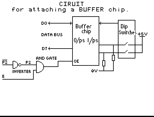
This could be used to read from a bank of DIP switches (an example circuit is shown in the following diagram). The chip may consist of 8 outputs (the data bus D0-D7) and 8 inputs (connecting to the DIP switches). The DIP switches when switched on connect to +5V, and when off are pulled down by the resistors to 0V. It has the power rails and two chip select lines (labelled OE1 & OE2). One of these lines can be connected to the Dragons P2 line to enable the device. However remember that the P2 line uses negative logic (ie a logic 1 state is 0V, and logic 0 is +5V) so first it must be fed through an invertor.

The important thing about interfacing these kind of devices is that the clock line (E) must also be connected. On the MC6821 there is a dedicated pin, on other devices you must decode the line yourself. In this case, the spare OE2 line can be connected to the E line- if you only have one chip select pin you need to AND the E line and P2 line together, before connecting it to the chip select pin.
If this circuit were connected to the Dragon, entering the command:
PRINT PEEK(&HFF40)
would display the settings of the DIP switches. Note in this instance we have not used the R/W line. This is because the buffer chip is read only, attempting a write (ie. a POKE) is meaningless. You can only READ the settings of the DIP switches.
There remains a problem in all this. Whether you are using a dedicated PIA or something like the buffer chip outlined above, you are limited to that one device. This device also happens to use the line that the disk systems uses. The problem lies in the P2 select line. You cannot simply connect all these devices to the same line. If you did, they would all be activated at the same time and try and read or write to the data bus, the result being somewhat of a mess.
In order to attach a number of devices to the Dragon, you will need to derive your own select lines, and leave the P2 for the disk system's use. In order to begin this, it is worth knowing a little about the Dragon's IO system.
The Dragon's IO is managed by the SAM chip. There are three separate chunks of memory dedicated to IO devices, and whenever an address in one of these chunks is present on the address bus (A0-A16) an appropriate P line is activated:
        P0 when $FF00 to $FF1F is requested.
        P1 when $FF20 to $FF3F is requested.
        P2 when $FF40 to $FF5F is requested.
P0 and P1 are connected to the 2 PIAs in the Dragon, and P2 as we are aware is brought out onto the cartridge port, and is used by the disk system. The important thing to realise, is the amount of effectivly unused space in this area. Refering back to the buffer chip example used earlier. This only requires 1 byte, yet the P2 line selectes the chip whenever you specify an address between $FF40 to $FF5F. So clearly, entering: PRINT PEEK(&HFF40), would have the same result as PRINT PEEK(&HFF41) or &HFF42,43 up to &HFF5F. All this space is wasted. It is the same with the Dragon's PIAs. These only use 4 bytes each, yet the P0 and P1 lines have 32 bytes each! You can see this for yourself, PRINT PEEK(&HFF20) should return the same as &HFF24, &HFF28... This is true also for the P0 area, EXCEPT on D64's where the serial chip appears at $FF04, so check this in steps of 8 ie. PEEK(&HFF00), &HFF08 etc.
Clearly, lots of the IO area is unused, filled up with redundant echoes of the internal PIAs. If these areas could be properly decoded, then they could be used for a number of devices you could add.
Having discovered the amount of redundant space in the Dragons IO areas, all that remains is to decode this in order to use the area for your devices. This requires some circuitry to look at the address bus, and when the address of your device appears, activate a signal to select your device. Before that however its worth mentioning the device types to use. If you take the lid of your Dragon off, and have a look at some of the smaller chips, you'll find a majority have the numbers 74LSxxxx on them. Taking a look in something like a Maplin catalogue, you will probably find most of these chips listed under Semiconductors section (the SAM chip also has a 74LS number, though its unlikely that will be listed). You'll also find listed, other 74 types including 74HC types. Its recommended that for all new designs, that 74HC chips are used. They are generally faster, and less current consuming than the old 74LS chips so it's worthwhile using these chips in your circuits.
Address decoding is relatively straightforward once you get the hang of it. First, decide which areas you want to use. For example if we use the unused areas at $FF10-$FF1F in the P0 area and $FF30-$FF3F in the P1 area for our devices. A PEEK or POKE to the areas will result in the address bus looking something as follows:
 A  A  A  A  A  A  A  A : A  A  A  A  A  A  A  A
16 15 14 12 11 10 09 08 :07 06 05 04 03 02 01 00
 1  1  1  1  1  1  1  1 : 0  0  ?  1  ?  ?  ?  ?

--this is the $FF part-- ---$10-$1F & $30-$3F---

   ? = varies
With this setup changing any of the A5 and A3-A0 lines will result in an address between $FF10-$FF1F or $FF30 to $FF3F.
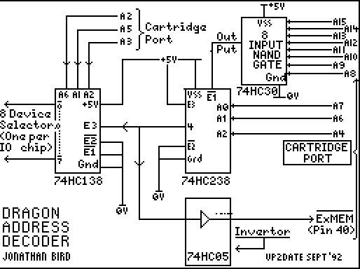
From this, I think its true to say, that the top 8 lines are always going to be set ie. $FF so we can decode these right away. Connecting all the lines to a 74HC70 8-input NAND gate should do the trick. This way, the output of the NAND will be low whenever the top 8 lines are $FF, and high at all other times. Next we have to be sure that A7 & A6 are 0 and A4 is 1. In order to do this we use a 3 to 8 decoder chip (74HC238). This chip has 3 inputs (labelled A0, A1 & A2) & 8 outputs (surprisingly enough). It takes a 3 bit binary number on the inputs, and activates one of the 8 outputs. So if:
A2 A1 A0
 0  0  0 in decimal 0, then 0 line is activated.
 0  0  1 in decimal 1, then 1 line is activated.
 0  1  0 in decimal 2, then 2 line is activated.


 etc. right up to 7.
Hence, connecting A7, A6 & A4 to the A0, A1 & A2 inputs of one of these chips, when A7 & A6 are 0 and A4 is 1:
A4 A6 A7
 1  0  0 in decimal 4, the 4 line is activated.
Connecting the output of the 8-input NAND gate used earlier to the E1 line of the decoder chip and connecting the remaining E lines so they are permanently enabled (E2 to 0V & E3 to +5V) will ensure that when we get a pulse on line 4 of the 3-8 decoder that an address in the range $FF10 - $FF1F or $FF30 - $FF3F has been requested. You could in fact use this line to enable your device, but it would only give 1 device select and its better to add the final decoder. How you do this can vary, but I've assumed that each device will require a maximum of 4 bytes each ie a PIA type device. The area we are using will therefore break down nicely into 8 4 byte slots. In order to do this, another 3 to 8 decoder can be used. This time connect the A5, A3 & A2 lines to its A2, A1 & A0 inputs. The A1 and A0 lines connect directly to the device as we have seen before to select internal registers. This chips needs its E1 enable line connected to the '4' output of the previous decoder, and the other E lines tied as before. The 0 to 7 output lines of this chip are your device enables. I suggest you use a 74HC138 decoder this time, since its outputs are inverted - giving you 8 P2 type chip selects. There remains one small problem. When your decoding selects its area, so does the Dragon's (ie. it activates a P0 or P1 line and enables an internal PIA). Fortunately there is a dedicated line on the cartridge port to stop this. Pin 40, labelled EXMEM will disable the internal selects, when pulled to 0V.
So when your device selects are activated (from pin '4' from the first 3-8 decoder) you will also need to connect this wire to the EXMEM line, but it will need to go through an invertor first.

Now you can attach your devices CS selects on the outputs of the 138 decoder. For example, if you had a PIAs CS line connected to pin 0 of the decoder, then it would appear at $FF10. Likewise something like the buffer chip connected to pin 1, at $FF14. Of course, since it only uses 1 byte, you would have 3 echoes at $FF15-$FF16 but its a distinct improvement over 32 echoes!
Once you have your address decode logic functioning, you are now in a position to begin expanding your machine's potential. You can also re-attach the DOS controller now that the P2 address select line has been freed up. Again, using a length of 40W ribbon cable, attach an IDC connector to one end and an IDC Edge Connector to the other. Using the spare socket on your expansion card re-connect the disk controller. Switch on, and all being well the DOS startup screen should be displayed.
(What to do when it goes wrong)
I can't think of any hardware I've ever built that has worked first time it's been plugged into the Dragon. Although the design may be theoretically sound, when it comes to wielding the soldering iron, there are countless unmentionable things that can go wrong. Unfortunatly most projects within magazines don't go into any depth about what to do when the circuit does not work. This is an attempt as a help on what to do when it goes wrong (& before it does).
I believe several episodes ago I suggested socketing all chips. That way the board can be initially soldered without chips on it reducing the risk of heat or static damage. Once the board has been soldering, check the underside for the obvious solder splashes across tracks, tracks cut in the correct place. In particular, if volts other than +5V from the computer are in use (the +12V line on the cartridge port for example) be sure that they do not connect with any of the CPU lines (address or data bus). They can withstand being pulled to +5V or 0V, but 12V (or -12/5V etc.) can cause serious damage. Check that all chips have power rails connected, and that the board has been cut underneath the chips themselves. I still fall into this trap quite often.
Once you have checked the board, plug in to the Dragon WITHOUT any chips present. When powering up the result, obviously should be nil. If the machine falls over (wavy lines on screen, nice hires screens etc.) then there is a solder fault. Unplug, and check the machine still works. Now its the tedious process of finding the fault(s). Obvious faults are processor control lines shorted to one another or +5V/0V. A multimeter on ohms range is invaluable here. If you can get the Dragon to behave without chips in the board, plug the chips in one at a time and power up each time checking for problems until all the chips are in. Remember, the usual handling procedure with chips (damage from static etc.) If you're building a largish board in stages, then obviously you do not need to remove chips that were put in earlier and you know work. For example, if the address decoding has been built (& tested to work) and you are merely adding a new device, then there is no need to remove the AD decode chips again. However it may be a good idea to remove chips if you are soldering very close to them. Useful test gear to have when debugging: a multimeter proves very useful, as does a logic probe capable of giving some indication of the fast pulses which are liable to be flying around your board.
Even if your board is functioning, there may still be unseen problems, external to this. Problems occur through the use of ribbon cable. I suggested the use of this cable to connect to the cartridge port, extra hardware boards and the disk controller. It is important to keep the length of this cable to a minimum. Ribbon cable, along with IDC connectors proves a flexible method of carrying large amounts of signals, unfortunatly it does have a high resistance, and things like stray capacitance/inductane and other such things that make you want to run away from it can occur. Processor signals are not particularly powerful, and can only travel a limited distance before falling over. Use of this cable should prove OK, but if you are planning further jumps of the cable of processor lines problems may lay in store. Warning signs of problems emerge through the disk system. When writing (& particularly formatting) disks the computer is under excessive strain. I went through a phase of being unable to format disks, and writing large files was susceptible to disk corruption. Formatting was accompanied with stray characters on the screen. The signs are, processor lines are giving out. Lines, in particular are the data bus, lower two address lines (A1 & A0 since these often feed to many chips containing registers PIAs, ACIAs), the R/W line & E line. I have recently encountered characters spuriously appearing on the screen on one of my Dragons for no apparant reason.
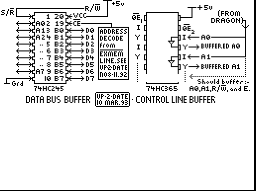
The answer to all this is to buffer the lines in question. For address lines, R/W & E lines a simple non-inverting hex buffer will suffice (eg 74HC365). As near as possible to the ribbon cable coming onto your board place one of these chips. Connect the line coming off the ribbon cable into the input of one of the buffers and the output to your device (eg. PIA, address decode etc.). The chip can be permanently enabled so tie the OE lines to 0V. This cured my disk problem, but if you still have problems it may be the data bus under strain. Buffering this is a little more tricky. The other processor lines (A0, A1, E etc.) are all one way ie. they come out of the processor to the device in question. However the databus allows signals in both directions, from the processor to a device and vice versa. Hence when buffering the data bus, the buffer needs to change direction. An ideal chip is a 74HC245 which buffers 8 lines in any direction and has a direction select (see diagram). This direction pin can be directly connected to the R/W line provided the processor side of the databus is connected to the 'B' side of the buffer, else the R/W line will need to be inverted. The DeltaDos disk controller in fact uses this method to buffer the data lines (the only disk card to buffer them).


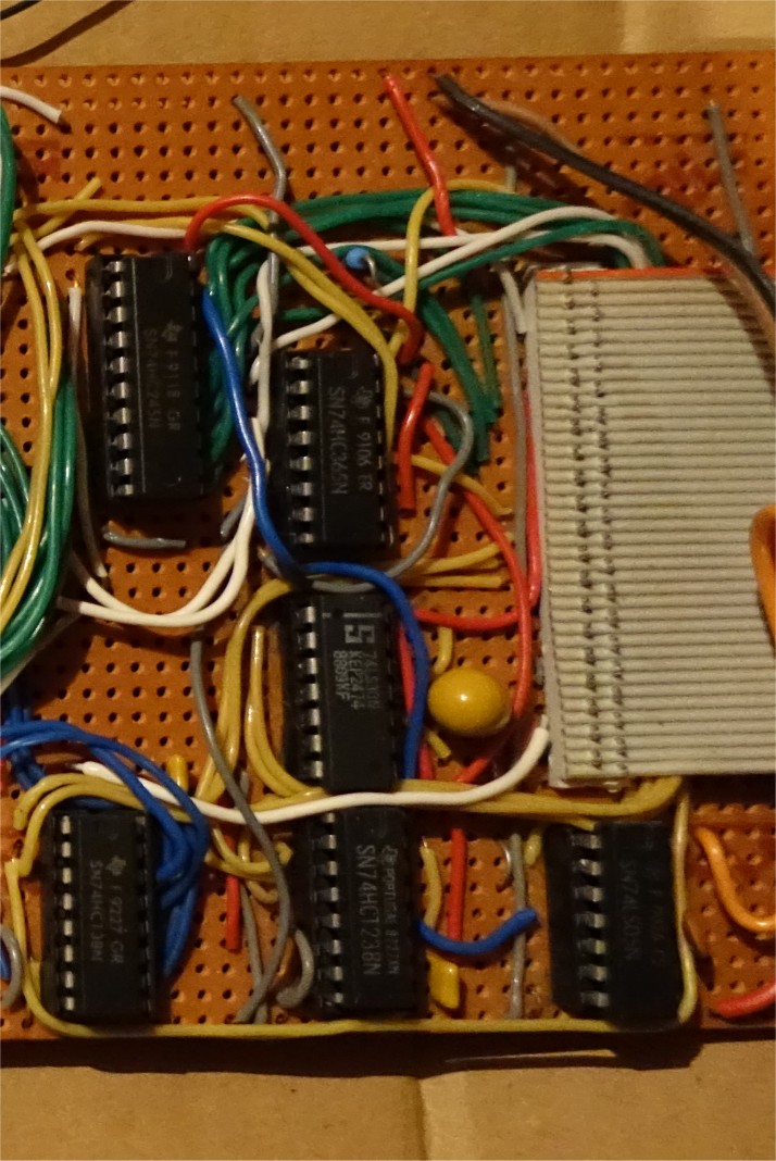
The address decode chips are the four at the bottom of this photo, whilst
the two at the top are the buffers. Later on I added an additional board
which sat between this and the cartridge edge connector which provided
buffering to all the key signals used.
The other possible area for problems is the power supply. I have not encountered problems with the power supply on any of my boards, but I may just be lucky. It's quoted in quite a few books, Dragon User's etc. that there is not a great deal of spare power available on the Dragon for add on bits. Running a disk system sucks a bit more out of it and I don't know what the limit is that the PSU can handle. In a letter from the editor of this wonderful disk(!) I was asked if I'd blown up a power supply yet, so I assume it must happen. Hopefully, by using as much CMOS (particularly HC devices) the power drain should be minimal. Try using the +12V line as much as possible (eg. for op-amps), since (particularly on the D64) this is not excessivly used. If you do loose a power supply, or the present one tends to play up then it may be worth replacing the thing with a good switched mode PSU (there were some ones going cheap at Greenweld a while back). I've bought one for my D64, but as yet haven't installed it. If you intend to opt for this approach, then beware - you'll need to wire up the mains side (all the usual rules apply - the chances are it'll need to be earthed) and re-wire the connector coming onto the main board, plus cut up the existing board to enable the modulator section to still be used. I'd only recommend this if you are adding some serious hardware or have existing problems. Having set that, with a good switched mode PSU you can probably run quite a lot - including the disk drives!
Addendum: The SMPS I eventually fitted to my D64 functioned perfectly, and had a number of unexpected side effects, noticably less display 'wobble' (the ripple effect that tends to occur across the screen and it also cured a long standing problem, that of the disk system not powering up properly. If this sounds familiar ie. the machine powering up and returning ?RF Errors or ?NR Errors on valid disks requiring a switch off/switch on sequence to sort it out then this may be the way to go.